BLOG
The Most Valuable Building on Earth
August 21, 2026 · Jonathan Godwin, CEO, Orbital Industries
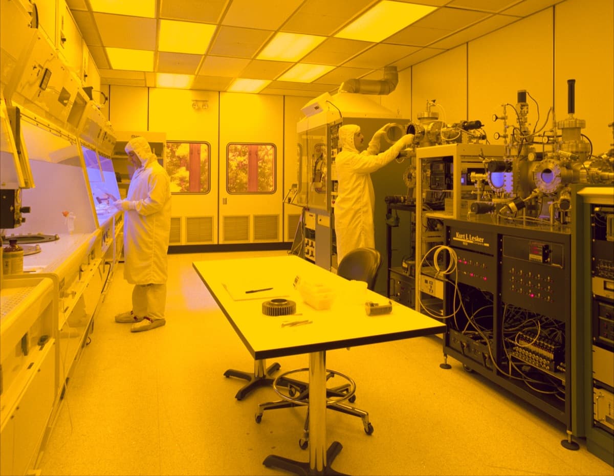
Photo: NASA Glenn Research Center
Elon Musk called Terafab "the largest and most valuable building on Earth." We can agree that he's right about the size, but whether it's valuable depends on whether anyone outside three companies can actually build one of these things.
Tesla and SpaceX are putting an initial $16.8 billion into Terafab, a semiconductor facility covering 100 million square feet in Grimes County, Texas, designed to combine logic, memory, packaging, and testing for use with robotaxis, humanoid robots, and space-based computing. Most news coverage has focused on the dollar funding amount in question; I want to focus on the building itself, because it's tricky to grasp what a fab actually has to do, and why it's so difficult.
What actually happens inside
Let's start with the wafer. First, a disc of silicon has to be purified to 99.9999% to 99.9999999%, so we're already starting at incredible constraints. Building a chip on it means repeating a handful of operations an enormous number of times, since material gets added in layers just a few atoms thick. A mask projects the circuit pattern through light onto a light-sensitive coating, and the exposed areas dissolve away. Impurities get implanted to change how the silicon conducts. The wafer is then subsequently heated above 1,000 degrees in order to repair that damage, and finally cooled down slowly to recover its crystal structure. The entire process is then carried out again on the following layer.
A logic chip runs this loop roughly 80 to 120 times, generating 500 to 1,000 process steps and around 90 masks over a three- to four-month cycle, with the wafer cleaned more than 200 times along the way, since any stray particle anywhere in that sequence can ruin the chip. A fab plant is essentially just this one loop involving clean, deposit, pattern, etch, clean, and measure.
Now if we were to compare this to a typical manufacturing plant, most of them have some built-in tolerance or allowance, so a component that's a little out of specification will still fit, or a slightly impure metal can still be used. But in the case of a modern chip, the features are measured in single-digit nanometres, so the process has to be accurate hundreds of thousands of times tighter than conventional manufacturing, with almost no room for drift. Just a few atoms in the wrong place or a tiny speck of invisible dust is enough to cause a step to fail and stop the chip before the process even fully begins.
This level of meticulousness has resulted in the industry spending decades chasing sources of interference nobody would even think to look for. Early researchers traced mysterious failures to workers who'd touched a copper doorknob, carrying enough stray atoms to contaminate machinery and chips. Intel later found that swapping in a slightly longer cable during construction could quietly degrade yield for months. Their fix was a practice called Copy EXACTLY, the idea being to build every new fab as a complete physical duplicate of one that already worked, right down to the exact paint used on the walls. That's the level of control a fab must maintain permanently, while still shipping hundreds of millions of chips a year.
The three companies that know how
Chip design is now "fabless", with companies such as Apple and Nvidia designing their own chips and then outsourcing the manufacturing to a foundry, since only a very small number of companies still attempt leading-edge nodes: the likes of TSMC, Samsung, and Intel. It takes decades to acquire the process knowledge needed to operate one of these facilities at a yield, and money alone doesn't provide a shortcut.
Even for the three companies that do know how to do it, the price of staying at the frontier keeps climbing. The same week Terafab made headlines, TSMC lifted its 2026 capex to $60–$64 billion, up from $52–$56 billion, and added $100 billion to its Arizona commitment, bringing the total there to $265 billion. All of this on the back of net income that was up 77.4% year over year.
The limitation in chip processing isn't demand; it's execution. Even if one had unlimited capital, a semiconductor fabrication plant would still be bottlenecked by a single company from the Netherlands. ASML is the sole maker of the EUV lithography machines that pattern advanced chips, and its newest High-NA systems cost $350 to $400 million each; a modern fab needs 9 to 18 of them. Each weighs 150,000 kilograms, ships in 250 crates, and takes six months and 250 engineers to assemble before running a single wafer. ASML builds only 12 to 15 a year, and yield learning after installation adds another 12 to 18 months before volume production starts. This is less a purchase order than a place in a queue behind every other advanced fab on Earth, for a machine that takes over a year to earn its keep.
Fifty picometers of margin
Once the tools are in, the room around them has to be cleaner and stiller than almost anywhere else humans build. Leading-edge cleanrooms run at ISO Class 4 or 5, permitting as few as 29 particles 0.5 microns or larger per cubic meter, versus over 3.5 million in a much laxer ISO 8 room, held by 300 to 480 full air changes an hour, replacing the room's entire air volume roughly every eight to twelve seconds. Even that isn't clean enough for the wafer, which travels between tools sealed inside pods, often entering an even cleaner sealed micro-environment than the room itself.
Underneath the cleanroom sits a sub-fab, one or two floors of pumps, chemical lines, and vacuum equipment that most visible tools depend on but that never appears on a factory tour, with an interstitial level above recirculating the air back down. Running through all of it is vibration control, an equally unforgiving standard: advanced EUV tools need vibration held below 50 picometers, a thousand times stricter than a decade ago, at a scale where a passing truck can ruin a wafer. The fix is entire rooms hung on isolation systems independent of the main structure, floating on elastomeric pads or springs. You're building a structure, then building several more inside it that aren't allowed to touch it. This holds even somewhere seismically calm like Texas, Arizona, or upstate New York, all preferred for new fabs for exactly that reason. The tools inside don't care whether vibration comes from a fault line or a passing train.
The constraints nobody sees
The sub-fab also contains the chemical stores, some of which are genuinely dangerous, such as toxic doping gases, and others that ignite on contact with air, all piped through stainless steel lines polished inside so they can't shed particles of their own. None of this is visible to a visitor, but a leak in this area can shut the entire factory down just as quickly as a problem in the cleanroom.
Above ground, water decides where a fab can be built. Every rinse needs ultrapure water, thousands of times cleaner than drinking water, with contamination held below 0.5 parts per billion at advanced nodes. A single leading-edge fab can use up to 10 million gallons a day, roughly what 33,000 US households use, and it takes 1,400 to 1,600 gallons of municipal water to produce 1,000 gallons of the ultrapure grade. Terafab's water will come from the Gibbons Creek Reservoir, built to cool a coal plant that shut in 2018, repurposing capacity that would otherwise sit unused.
Beneath all this is a power supply that cannot fail for even a fraction of a moment. A voltage dip lasting just 10 to 20 milliseconds can ruin an entire in-process wafer lot, since a wafer mid-fabrication can't be paused and resumed. Fabs aim to counteract this by layering redundant substations, battery storage, and diesel generators under their UPS, but even then, they can still get caught out. TSMC's own Fab 21 in Arizona lost hours of production to a disruption traced to an external gas supplier, not even its own grid connection. A single unplanned hour of downtime at a leading fab runs $2 to 5 million in lost production, before scrapped lots or recalibration.
The part nobody can predict
By now, the shape and complexity of the problem should be clear. A wafer has to survive a hundred repetitions of a process with almost zero tolerance for error, in a room stiller than the ground beneath it and thousands of times cleaner than the air outside it, fed by chemicals that can ignite on contact with air. All of this topped off by a power supply that can't blink for a fraction of a second, water purer than anything in nature, and a process using machines only one company on Earth can build.
A fully in-house, end-to-end process is a genuine solution to a real problem: logic, memory, packaging, and testing under one roof means fewer places for one vendor's delay to become everyone else's problem. However, owning the loop doesn't make it smaller. Every discipline in this piece, from lithography and cleanroom control to chemical handling, water supply, and power resilience, still has to hold at the same tolerance, in the same building, for the entire life of the fab.
The part that no one can predict now is whether Terafab can keep to all of those constraints on the same site for a number of years.